
Photolithography/Mask Aligner/Nanoimprinter Lithography
Note: This system supports both conventional photolithography (mask aligner mode) and nanoimprint lithography (NIL) capability. Standard operation described below focuses on photolithography workflows. NIL-specific processes may require additional protocols and training.
Model: Neutronix-Quintel NXQ4006
Neutronix-Quintel NXQ4006 USER MANUAL
SOP for Photolithography and Mask Aligner
Pattern transfer process using UV exposure and photoresist development. Combines spin coating, mask alignment, and controlled exposure for microfabrication. Supports high-resolution device fabrication.
Location: SE1 154 (cleanroom Class 100)
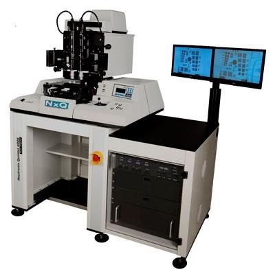
Supports soft contact, pressure/hard contact, vacuum contact, and proximity modes. The aligner can be lifted with an accessory feature that permits proximity printing in addition to the contact printing modes.
Photoresist Data Sheets
MICROPOSIT S1800 SERIES PHOTORESISTS
SU-8 Permanent Negative Epoxy Photoresist 2-25
SU-8 Permanent Negative Epoxy Photoresist 50-100
Literature
Micron Fabrication – Intro to Photolithography
Introduction to Photolithography By Nanolink
Photolithography Solvent Based by Nanolink
Photolithography Source: Dr. R. B. Darling (UW) lecture notes on photolithography
Nanoimprint Lithography (NIL) Capability
The system includes (or is being configured to include) nanoimprint lithography (NIL) capability for high-resolution pattern transfer beyond conventional photolithography limits.
NIL enables patterning by mechanically imprinting nanoscale features into a resist layer, followed by curing (thermal or UV depending on process).
Key Differences from Photolithography:
- No photomask exposure required in the traditional sense
- Direct physical pattern transfer using a mold/stamp
- Capable of sub-100 nm (and below) feature sizes
- Requires specialized resist materials and process conditions.
Important Note:
NIL processes require:
-
Dedicated training
-
Specific materials (imprint resists)
-
Process-specific parameters (pressure, temperature, curing conditions)
Users must consult SCIF staff before attempting NIL processes.
Photolithography System (Mask Aligner + Photoresist Processing)
The photolithography process at SCIF utilizes a mask aligner system (Neutronix-Quintel NXQ4006) in combination with MICROPOSIT® S1800 series positive photoresists for pattern transfer onto substrates. This process enables fabrication of micro- and nano-scale features through controlled UV exposure and chemical development.
Key Components
- Mask aligner (NXQ4006 UV exposure and precision alignment system)
- Spin coating system for photoresist application
- Hotplates for soft bake and post-bake
- MICROPOSIT® S1800 series photoresists (e.g., S1813)
- Developer solutions (e.g., MF-319, MF-321)
Mask Aligner Process Flow
Users are expected to follow a structured workflow when operating the mask aligner (NXQ4006), as this step is critical to pattern transfer accuracy and device quality.
Pre-Alignment Preparation
Users are expected to ensure that the substrate has been properly cleaned, dehydrated, photoresist-coated, and soft baked. The wafer should be cooled before alignment. The photomask must be clean, defect-free, and correctly oriented. Both wafer and mask surfaces must be inspected for particles or contamination.
System Setup
The UV lamp must be warmed up (approximately 15-20 minutes) prior to exposure. Users must verify that the vacuum system for both wafer chuck and mask holder is functioning properly. The stage, chuck, and mask holder must be clean and free of debris. Appropriate exposure and alignment modes must be selected before proceeding.
The NXQ4006 system provides improved exposure uniformity and programmable control of exposure parameters (time and intensity), enabling more consistent pattern transfer across the substrate.
Wafer and Mask Loading
The wafer must be placed securely on the vacuum chuck, and vacuum engagement must be confirmed. The mask must be carefully loaded onto the mask holder without introducing contamination. Users must ensure proper positioning and visibility of alignment marks.
Alignment Procedure
Alignment is performed using the microscope system. Users are expected to carry out coarse alignment followed by fine alignment, ensuring accurate matching of alignment marks. Careful and deliberate alignment is required to prevent pattern misregistration.
The NXQ4006 provides enhanced microscope optics and precision stage control (X, Y, Theta) for improved alignment accuracy.
Contact and Exposure
Users must select the appropriate contact mode (soft contact, pressure/hard contact, vacuum contact, and proximity mode) based on process requirements. Before exposure, users must verify contact conditions, alignment accuracy, and exposure parameters (dose/time and wavelength). Exposure should only be executed after all conditions are confirmed and system interlocks are properly engaged.
The system supports high-uniformity UV exposure (typically 350–450 nm, commonly optimized near 365–436 nm depending on lamp configuration).
Post-Exposure Handling
After exposure, users must carefully release vacuum and remove the wafer without disturbing the patterned resist. The wafer should then proceed to post-exposure bake (if required) and development. Proper handling must be maintained to avoid contamination.
Cleanup and System Readiness
Users are expected to clean the chuck, mask holder, and surrounding workspace after use. All materials must be removed, and the system must be left in a clean and ready condition for the next user. Usage logs must be completed as required.
Critical Expectations
Users must verify all process settings before exposure, handle masks and wafers with care, and avoid forcing any mechanical components. Safety interlocks must never be bypassed. Maintaining cleanliness and process control is essential to achieving reliable results.
Photolithography Workflow
- Substrate cleaning and preparation
- Photoresist coating (spin coating for uniform thin films)
- Soft bake (typically ~115°C for ~60 seconds)
- Mask alignment using optical microscope
- UV exposure (typically in 350–450 nm range, optimized near 365–436 nm depending on lamp configuration)
- Development using compatible developer solutions
- Post-processing (hard bake or additional steps as required)
Mask Aligner Operation (NXQ4006)
- UV lamp requires warm-up (~15-20 minutes) before exposure
- Mask and wafer are secured using vacuum chuck systems
- Alignment performed using microscope (single-field or split-field modes)
- Contact modes include soft contact, pressure/hard contact, vacuum contact, and proximity mode
- Exposure executed after alignment verification
- System includes interlocks for vacuum, pressure, and positioning
-
Programmable exposure control with improved repeatability and uniform illumination across the exposure field
Process Characteristics
- Film thickness controlled by spin speed (typically optimized between ~1000–3000 rpm)
- Photoresists provide uniform, high-resolution coatings with good adhesion
- Capable of sub-micron resolution (down to ~0.5 µm features under optimized conditions)
- Compatible with a range of substrates and exposure conditions
Training and Usage
Users are trained on:
- Photoresist handling and coating techniques
- Mask alignment procedures and exposure modes
- Process parameter selection (dose, time, development)
- Cleanroom safety and chemical handling
Safety Considerations
- Photoresists are chemical substances requiring proper PPE (gloves, goggles, ventilation)
- UV exposure systems require eye and skin protection
- Proper handling of solvents and developers is required
- Equipment must be operated within specified vacuum and pressure conditions
Detailed Safety Considerations
The photolithography system involves hazards associated with UV radiation, moving mechanical parts, vacuum/pressure contact operation, hot surfaces, and chemical exposure. Only trained and authorized users may operate the mask aligner, spin coater, hotplates, and associated chemical-processing equipment. Facility SOPs and the current SDS for all photoresists, developers, and solvents must be reviewed before use.
UV Exposure Safety
The mask aligner uses a high-intensity UV source for exposure. Direct or reflected UV light can injure the eyes and skin. Never bypass covers, shields, or interlocks during operation. Confirm that the exposure area is closed and secured before starting exposure. Avoid looking into the optical path or exposure source under any condition. Allow the lamp to warm up only according to procedure, and do not attempt maintenance or lamp access unless specifically authorized.
Vacuum, Contact, and Mechanical Hazards
The mask aligner uses vacuum chucks and contact modes including soft contact, pressure contact, vacuum contact, and proximity printing. Improper loading, unloading, or contact setting can crack masks, damage wafers, or create pinch hazards around moving stages and lift mechanisms. Users must verify mask placement, wafer placement, chuck vacuum, and selected contact mode before alignment or exposure. Hands must be kept clear of moving assemblies during loading, alignment, and contact engagement. Do not force any component or attempt manual adjustment while the system is under vacuum or in motion.
Chemical Safety: Photoresists
MICROPOSIT S1800 series photoresists are combustible mixtures and may irritate the eyes, skin, and respiratory system. Vapors and mists should not be inhaled. Handle photoresists only in approved ventilated areas such as designated chemical hoods or exhaust-equipped processing stations. Wear appropriate chemical-resistant gloves, splash goggles, and suitable protective clothing. Remove contaminated gloves immediately and wash hands thoroughly after handling. Keep photoresists away from heat, sparks, flames, and other ignition sources.
Chemical Safety: Developers
Developer solutions such as MF-319 can cause irritation and may contain hazardous alkaline components including tetramethylammonium hydroxide. Avoid skin contact, eye contact, ingestion, and inhalation of mist. Use only in approved wet-processing areas with proper ventilation and chemical controls. In the event of contact, immediately flush the affected area with water and follow facility emergency procedures. Treat all developer spills as chemical incidents and respond according to cleanroom spill protocol.
Hotplate and Thermal Safety
Soft-bake and post-bake steps involve hot surfaces that can cause burns and may increase solvent vapor release from coated substrates. Use wafer tweezers or approved handling tools when loading or unloading hotplates. Never place combustible materials near heated equipment. Allow substrates to cool in designated areas before transport to the aligner or developer station.
Ventilation and Exposure Control
Spin coating, resist dispensing, edge-bead removal, developing, and solvent rinsing must be performed only in designated process areas with proper exhaust ventilation. Containers should remain closed when not in use. Dispense the minimum amount needed for the process. Do not leave uncapped chemical bottles or waste containers open in the cleanroom.
PPE Requirements
Minimum PPE for routine operation includes cleanroom garments required by the facility, safety glasses or chemical splash goggles as appropriate, and chemical-resistant gloves compatible with the chemicals in use. Additional face protection may be required when handling developers or transferring chemicals in larger volumes. Gloves exposed to photoresist, developer, or solvent must not touch door handles, keyboards, microscope controls, or common-use surfaces. Replace gloves immediately if contaminated.
Operational Controls
Before operation, verify:
- the correct mask and substrate are clean and dry,
- vacuum lines and contact settings are correct,
- the lamp warm-up and exposure settings are appropriate,
- the chuck, mask holder, and microscope area are free of debris,
- waste containers are available and properly labeled,
- the user log and process log are completed as required.
Waste Disposal
Photoresist, developer, contaminated wipes, solvent rinses, and disposable lab materials must be collected in designated labeled waste containers. Do not pour developer, resist, or solvent waste into sinks or drains. Segregate waste streams according to facility chemical waste rules and notify staff when containers are nearing capacity.
Emergency Response
In case of chemical splash, immediately use the nearest eyewash or safety shower as appropriate and notify cleanroom staff. In case of UV system malfunction, unusual odor, vacuum failure, mask breakage, or abnormal equipment motion, stop the process if safe to do so, secure the tool, and report the issue immediately. Do not resume operation until the equipment has been evaluated and cleared.
Good Cleanroom Practice
Use only approved materials and recipes. Keep masks, wafers, and chuck surfaces free of particles. Clean the workspace after use, remove all sample debris, and leave the aligner, spin area, and bake stations in ready condition for the next user. Report damaged masks, vacuum leaks, lamp instability, and process irregularities promptly.
WAFER CLEANING PROTOCOLS
Wafer Cleaning Protocol for SCIF Cleanroom
Hot Bath Cleaning Protocol (Wet Bench Cleaning)
Wafer Cleaning (Simple Cleanroom Method)
Photolithography Training – Session Coverage
During the training session, the following topics and steps will be covered:
-
Overview of photolithography process and workflow
-
Cleanroom safety, PPE, and chemical handling
-
Substrate preparation and wafer cleaning basics
-
Photoresist handling and spin coating techniques
-
Soft bake and post-bake processes
-
Mask aligner operation (alignment, contact modes, exposure)
-
Exposure parameters (dose, time, wavelength considerations)
-
Development process and rinsing
-
Inspection of patterned features
-
Common process errors and troubleshooting basics
-
Proper cleanup procedures and waste disposal
Training is conducted using standard samples and facility-available photoresists, focusing on safe operation and understanding of the complete process flow; users are responsible for carrying and advancing their own research projects.
